HY1602 is an intelligent digital multi-mode Flyback controller. The newly developed architecture supports Constant Voltage (CV), Constant Current (CC) and over load (LPS) for maximum 64ms.
HY1602 integrates rich protections and features such as line compensation, slope compensation, transformer short protection, output over-voltage protection, over-temperature protection, brown in and brown-out, sense resistor short protection. HY1602 has 4 options: HY1602A (65kHz, CV/LPS, on chip OTP), HY1602B (89kHz, CV/LPS, on chip OTP), HY1602C (65kHz, CV/LPS, on chip OTP and external NTC OTP), HY1602D (89kHz, CV/LPS, on chip OTP and external NTC OTP).
HY1602 is available with the SOT23 package.
· Intelligent Digital Multi-Mode Control
· Peak Current Mode Control at Burst-Mode /PFM/DCM/CCM
· Continuous-Conduction Mode (CCM) at Low Line(LL), QR at High Line(HL) to Balance the Switching Loss and the Conduction Loss
· Over-load Period up to 64mS (option)
· Output Constant Current Regulation
· Switching Frequency Dithering to Improve EMI
· Adaptive MOSFET Gate Drive to Balance Switching Loss and EMI
· MOSFET Gate Voltage is Clamped at 12V
· Rich Protection Features
§ Output OVP with Latch
§ VCC OVP with Latch
§ Transformer Saturation Protection
§ Output Short Circuit Protection
§ Current Sensor Resistor Short Protection
§ Output Open Loop Protection
· Line Feed-forward Compensation
· Brown-in and Brown-out
· Power Consumption < 75mW
· Low Start-up Current (<3µA)

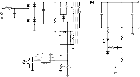
Fig 2. Typical Application Circuit
| Version | HY1602A | HY1602B | HY1602C | HY1602D |
|---|---|---|---|---|
Feature | CV/CC/LPS | CV/CC/LPS | CV/CC/LPS | CV/CC/LPS |
Operation Mode | No-Load: Burst LL: DCM/CCM HL: QR | No-Load: Burst LL: DCM/CCM HL: QR | No-Load: Burst LL: DCM/CCM HL: QR | No-Load: Burst LL: DCM/CCM HL: QR |
Switching Frequency | LL: 65 kHz HL: 65 kHz | LL: 89 kHz HL: 89 kHz | LL: 65 kHz HL: 65 kHz | LL: 89 kHz HL: 89 kHz |
| VCC | POR: 16V UVLO: 7.5V | POR: 16V UVLO: 7.5V | POR: 16V UVLO: 7.5V | POR: 16V UVLO: 7.5V |
Adaptive Driver (*) | Adaptive Drive 12V | Adaptive Drive | Adaptive Drive | Adaptive Drive |
Output Peak Current Period | 64ms | 64ms | 64ms | 64ms |
Line Voltage Sens | Yes | Yes | Yes | Yes |
Brown-in/Out | Yes | Yes | Yes | Yes |
Frequency Jittering | +/- 10% | +/- 10% | +/- 10% | +/- 10% |
Protection | ||||
Vout_OVP | 3.95V(Latch) | 3.95V(Latch) | 2.5V(Latch) | 2.5V(Latch) |
Transformer Saturation Protection | Yes | Yes | Yes | Yes |
Open Loop Protection | Yes | Yes | Yes | Yes |
Current Sense Short Protection | Yes | Yes | Yes | Yes |
Thermal Shutdown (*) | Yes On chip OTP | Yes On chip OTP | Yes On chip OTP & external NTC OTP | Yes On chip OTP & external NTC OTP |
VCC OVP | 26V | 26V | 26V | 26V |
*:Patented Technology
| 標題 | 最後更新 | 分享 | 觀看次數 |
|---|
(TOP VIEW)

SOT23-6
No. | Name | Description |
1 | GND | Ground. |
2 | FB | Voltage loop feedback input. Connect an opto-coupler from the FB pin. |
3 | VMS | Auxiliary winding detection signal input. It detects the input voltage and output voltage information |
4 | CS | Current sensing input. |
5 | VCC | VCC is the supply of IC. The controller is enabled when VCC voltage reaches VCC_ON and disabled when VCC drops below VCC_UVLO. |
6 | OUT | Gate drive output and NTC detection input |
版權所有©2020 華源智信半導體(深圳)有限公司│粵ICP備20068124號