
The ANX7911 outputs 14 voltage references for Gamma correction in TFT-LCD displays and one voltage reference for Vcom. Each reference
voltage whether for Gamma or Vcom has its own 10-bit digital-to-analog converter (DAC) and
amplifier to ensure a stable voltage when critical levels and patterns are displayed.
The ANX7911 also has integrated multiple-time programmable (MTP) memory to store Gamma and Vcom values on the chip, eliminating the need for external EEPROM. ANX7911 supports up to 1000 write operations to the on-chip non-volatile memory.
The Gamma outputs can settle within 1us. The Vcom output can provide 100mA peak transient current and also settles within 1us. The analog supply voltage range extends from 6.5V to 18V, and the digital supply voltage range extends from 2.7V to 3.6V.
Gamma values and the Vcom value are programmed into registers through the I2C interface.
The ANX7911 is available in a thin 32-pin 5x5 mm WQFN green package.
l 6.5V to 18V input supply
l 14-channel rail to rail programmable Gamma Buffers
- 10 bits resolution for each channel
- 25mA output current for each channel
- 2 banks register using BANK_SEL to select which bank data output
l 1-channel rail to rail operational amplifier
- 7 bits adjustable output
- ±100mA Output Current
- ±140mA Output Short-Circuit Current
- 20V/μs Slew Rate
l 2-wire I2C slave mode interface
l One control pin to allow storing data into NVM (Non-Volatile Memory)
l Thermal shutdown
l Thin 5x5 mm 32-lead WQFN package
PIN CONFIGURATION

| 标题 | 最后更新 | 分享 | 观看次数 |
|---|
ORDERING INFORMATION
| Part Number | Package |
|---|---|
ANX7911AAQ | WQFN-32L, 5x5 |
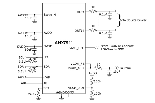
TYPICAL APPLICATION DIAGRAM

版权所有©2020 华源智信半导体(深圳)有限公司│粤ICP备20068124号


